The surfaces of materials possess unique characteristics that can be applied to create novel functional properties. Our research seeks to create nanostructured surfaces and thin films with novel electronic/magnetic functions. We also pursue experimental and theoretical analyses of the processes by which such surfaces and thin films are formed to explore potential applications in advanced devices and systems.
(1) Creating nanostructured surfaces and thin films with novel electronic/magnetic functions
We are using electrochemical processing, such as electrochemical and electroless deposition processes, electrochemical etching, and self-organized organic monolayers, to develop new processes for fabricating nanostructured surfaces. We also use photolithography, electron beam lithography, and nano imprinting, etc., to obtain arrayed nanodots, high aspect ratio pores, and so on.
(2) Analysis and modeling of nanostructure fabrication processes at the solid/liquid interface
Our work in this area includes ex situ and in situ analyses of reaction processes; computer simulations of processes using molecular orbital (MO) and density functional theory (DFT) approaches; and development of new methods to assess the structural and functional properties of nanostructured surfaces on a nanometer scale, primarily by scanning probe microscopy. SPM includes scanning tunneling microscopy (STM), atomic force microscopy (AFM), scanning surface potential microscopy (SPoM), tunneling AFM (TAFM), and magnetic force microscopy (MFM).
(3) Developing advanced devices and systems
Applying the functional surfaces and thin films developed as described above makes it possible to devise advanced devices, including ordered arrays of magnetic nanodots, so-called “bit patterned media” for ultra-high-density data storage devices, picoliter-volume glass tube arrays for micro reactors, and highly-sensitive sensing devices for X-ray imaging and immunoassays.
(4) Analysis of Si wet device processes; developing new nanofabrication processes
Wet (chemical) processes have played a key role in Si device manufacturing, and a precise process has now been developed. Certain mechanisms, however, including reactions at the solid/liquid interface, have yet to be fully understood. We are using the analytical approaches described above to investigate Si device processes, including the preparation of ultra-clean surfaces, and the nanostructuring of Si wafer surfaces to achieve an atomistic understanding of silicon surface chemistry under device processing.
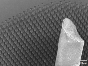
Fig 1 CoPt ferromagnetic nanodot array for ultra-high-density magnetic data storage devices.
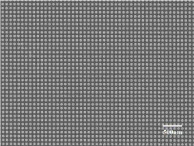
Fig.2 Array of 3D microelectrodes for electrochemical microreactor.
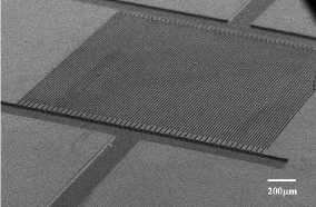
Fig.3 Electrochemical micro reactor system containing the array electrode shown in Fig. 3.
B.S. Waseda University (1987); Ph.D, Waseda University (1992); Assistant Professor(1993-1996) and Associate Professor(1996-2005), Waseda University; Visiting Associate Professor, Stanford University (1997-1998); Principal Investigator, NSF I/UC Research Center for Silicon Wafer Engineering and Defect Sciences (1998-present); Associate Editor of Journal of The Electrochemical Society (2003-present), Chair of Division 5, International Society of Electrochemistry (2011-present). Award for Young Scientists, Electrochemical Society of Japan (1999); Best Paper Award, International Union of Surface Finishing, (2000); Research Award, The Electrochemical Society (2010), Research Paper Award, The Electrochemical Society of Japan (2013).